Lead beneficiary:
École Polytechnique Fédérale de Lausanne (EPFL)
Participants:
Université de Technologies de Troyes (UTT)
Université de Bourgogne (UBT & UBE)
Teem Photonics (TP)
University of Oxford (UOXF)
QuTools GmbH (QuT)
Aurea (AU)
Enhancing the light-matter interaction at single-atom/photon level is required for quantum technologies. The coupling strength depends on the quality factor Q and effective volume V of the involved mode by the ratio Q/V. High and efficient light matter interaction can be achieved in cavity-based systems (see WP1 and WP2). In this WP, we will transpose quantum optics techniques to nanophotonics using hybrid plasmonic-photonic nanostructures taking benefit of sub-wavelength dimension. Surface plasmon polaritons (SPP) (modes sustained by metallic nanostructures) present low mode volumes and can interface light and matter at the nanoscale. We propose to use innovative photonic structures with quantum emitters [quantum dots (QDs) and nitrogen-vacancy centres in nanodiamonds (NDs)], embedded in 1D and 2D photonic waveguides (WGs). They will be either coupled to hybrid metallic-dielectric WGs (UBE), to dielectric-only WGs but with an elaborate ‘double’ photonic structure (EPFL) or to nanoplasmonic cavities for CQED-type experiments (UTT).
UBE demonstrated i) high Purcell factor (~20) for a single photon source to a plasmon slot WG (see Figure 2a) and ii) efficient emission coupling (~45%) from a cluster of QDs into a TiO2 photonic WG, mediated by plasmon lensing from a metal film [ACS Phot. 3, 844 (2016)]. We will combine these two approaches to couple the emission of a single QD into the photonic guide, as a step towards an integrated quantum photonic platform. We will replace the metal film by the slot WG in the hybrid plasmonic-photonic platform (HPP). Single photon circuitry will be designed shaping the metal/TiO2 interface. In order to improve further the light/matter interaction, UBE, UTT, EPFL, and TP will use experimental configurations for high confinement such as a metallic slit coupled to a dielectric WG [Nano Lett. 10, 2922 (2010)], a funnel-type plasmon cavity made of concentric rings [Appl. Phys. Lett. 94, 51105 (2009)] and an integrated Yagi-Uda optical antenna. UTT designed a double bowtie nanoantenna leading to a Purcell effect and a single ND was successfully inserted at the center of the structure (Figure 2b). EPFL has developed the growth of a single photon source within a nanowire (NW) showing a good photonic structure (Figure 2c) [Nature Materials 12, 439 (2013)]. This will be combined with the work of UTT, where a single photon source was excited by a single NW WG of high index [Sci. Rep. 6, 19721 (2016)], for more mature integrated optical WGs. EPFL also demonstrated directional emission for the semiconductor nanowire feeding a Yagi-Uda plasmonic antenna [Nano Lett. 15, 4889 (2015)]. This will be also implemented for directionnal coupling into the HPP platform at UB.
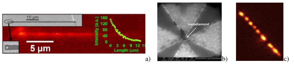
a) Single QD coupled to a slot Au waveguide. The mode propagation along the slot is visible (inset: QD within the slot). b) Double bowtie structure as a nanocavity with a single ND placed in the center (scale bar: 1 μm). c) Panchromatic cathodoluminescence map of a 2μm nanowire with QDs reveals their nano-localisation.
We also want to use mature results in CQED in order to obtain important breakthroughs by connecting the quantum optics and nano-optics communities. UBT&E and UTT very recently developed an original formalism that directly transposes CQED concepts to localized SPP [Phys Rev. B 93, 045422 (2016); Phys. Rev. A 94, 023818 (2016); Opt. Lett. 41, 4480 (2016)]. UBT&E and UTT will adapt the formalism to configurations with delocalized plasmon (in WG) and integrated photonics in order to describe the devices investigated by UBE, UTT and TP.
WP 4 aims at the transfer of atom/ion-cavity schemes to nano-scale light-matter interaction. UBT&E, UTT, UOXF and UoS will transpose the general CQED description to the plasmon-atom coupled system in order to gain an insight into the coupling mechanism and taking into account the strong losses in the metal. Conditions to achieve the strong coupling regime at the single photon/single plasmon level would be an important breakthrough. EPFL, UTT and UBE in cooperation with the industry teams TP and AU, will develop challenging experiments involving emitter-plasmon coupling. Three complementary approaches will be considered: UBE (with EPFL) for the integration of solid-state sources in a HPP platform, UTT with emitters coupled to a high quality optical waveguide (specifically provided by TP) via a plasmonic cavity, and EPFL (with TP and UTT) will work towards a ‘double’ photonic structure, a single photon source from a QD within a nanowire grown by epitaxy and coupled to an integrated optical waveguide. This very novel approach uses the intrinsic properties of the as-grown quantum-emitter-in-a-nanowire system. In all cases, we anticipate an efficient emission in the optical guide due to the plasmonic structure. Four ESRs will be mainly assigned to WP 4.